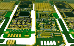
Effective PCB routing is a cornerstone of successful circuit board design, playing a crucial role in enhancing the overall performance of the device. It involves the strategic placement of copper traces to connect different components on a board. When done correctly, it ensures optimal signal integrity, reduces electromagnetic interference (EMI), and enhances the electrical performance of the PCB.
Minimizing Signal Degradation
One of the primary benefits of effective PCB routing is the minimization of signal degradation. In high-frequency circuits, improper routing can lead to significant losses in signal strength and integrity. For instance, a poorly routed high-speed signal, such as those exceeding 1 GHz, can suffer from attenuation or signal loss as much as 3 dB per meter, which can cripple the functionality of the device. Effective routing ensures that signal paths are as short and direct as possible, reducing the risk of signal degradation due to length and avoiding cross-talk with other signals.
Optimizing Power Distribution
Effective routing also involves the careful management of power distribution across the PCB. This includes designing power planes that provide stable and low-impedance sources to all components on the board. Inadequate power distribution can lead to voltage drops and fluctuating power supply that can affect the performance of sensitive components. By implementing strategies such as using thicker traces for power lines, or designin
g specific paths for power and ground planes, designers can ensure a more reliable and stable operation.
Reducing Electromagnetic Interference (EMI)
EMI can severely disrupt the performance of a PCB, especially in environments with numerous electronic devices. Effective PCB routing can mitigate EMI by strategically placing sensitive signals away from potential sources of interference and by using techniques such as differential signaling. Proper separation and shielding techniques, when combined with thoughtful layout planning, can reduce the susceptibility of a PCB to external and internal noise, thereby improving its performance and reliability.
Enhancing Thermal Management
The layout of traces can significantly impact the thermal performance of a PCB. Effective routing contributes to better heat distribution across the board, preventing hot spots that can damage components. By using thermal vias and placing heavier traces in heat-prone areas, designers can help dissipate heat more evenly. This not only prevents thermal issues but also enhances the longevity and reliability of the device.
Improving Manufacturing Yields
Well-planned PCB routing simplifies the manufacturing process, leading to higher yields and lower costs. Complex or poorly designed routes can cause issues during the PCB fabrication and assembly stages, such as incomplete etching or difficulties in component placement. By adhering to design standards and ensuring routes are easily accessible and manufacturable, designers can reduce errors and improve the overall quality of the final product.
Facilitating Easier Testing and Maintenance
Lastly, effective routing can make the PCB easier to test and maintain. Logical and clear routing simplifies the process of debugging and tracing faults within the circuit. It also makes it easier for technicians to perform repairs or upgrades, as components and their connections are more accessible.
Effective PCB routing is more than just connecting components; it’s about enhancing the PCB’s functionality, reliability, and efficiency. By prioritizing good routing practices, designers can ensure their PCBs perform optimally under various conditions, providing a robust foundation for the functionality of the electronic device.